- 您现在的位置:买卖IC网 > Sheet目录3753 > ATMEGA169P-16MCHR (Atmel)MCU AVR 16KB FLASH 16MHZ 64-VQFN
PIC16F946
DS41265A-page 150
Preliminary
2005 Microchip Technology Inc.
12.1
A/D Configuration and Operation
There are three registers available to control the
functionality of the A/D module:
1.
ANSEL (Register 12-1)
2.
ADCON0 (Register 12-2)
3.
ADCON1 (Register 12-3)
12.1.1
ANALOG PORT PINS
The ANS<7:0> bits (ANSEL<7:0>) and the TRIS bits
control the operation of the A/D port pins. Set the
corresponding TRIS bits to set the pin output driver to
its high-impedance state. Likewise, set the correspond-
ing ANSEL bit to disable the digital input buffer.
12.1.2
CHANNEL SELECTION
There are up to eight analog channels on the PIC16F946,
AN<7:0>. The CHS<2:0> bits (ADCON0<4:2>) control
which channel is connected to the sample and hold
circuit.
12.1.3
VOLTAGE REFERENCE
There are two options for each reference to the A/D
converter, VREF+ and VREF-. VREF+ can be connected to
either VDD or an externally applied voltage. Alternatively,
VREF- can be connected to either VSS or an externally
applied voltage. VCFG<1:0> bits are used to select the
reference source.
12.1.4
CONVERSION CLOCK
The A/D conversion cycle requires 11 TAD. The source
of the conversion clock is software selectable via the
ADCS bits (ADCON1<6:4>). There are seven possible
clock options:
FOSC/2
FOSC/4
FOSC/8
FOSC/16
FOSC/32
FOSC/64
FRC (dedicated internal oscillator)
For correct conversion, the A/D conversion clock
(1/TAD) must be selected to ensure a minimum TAD of
1.6
selected frequencies.
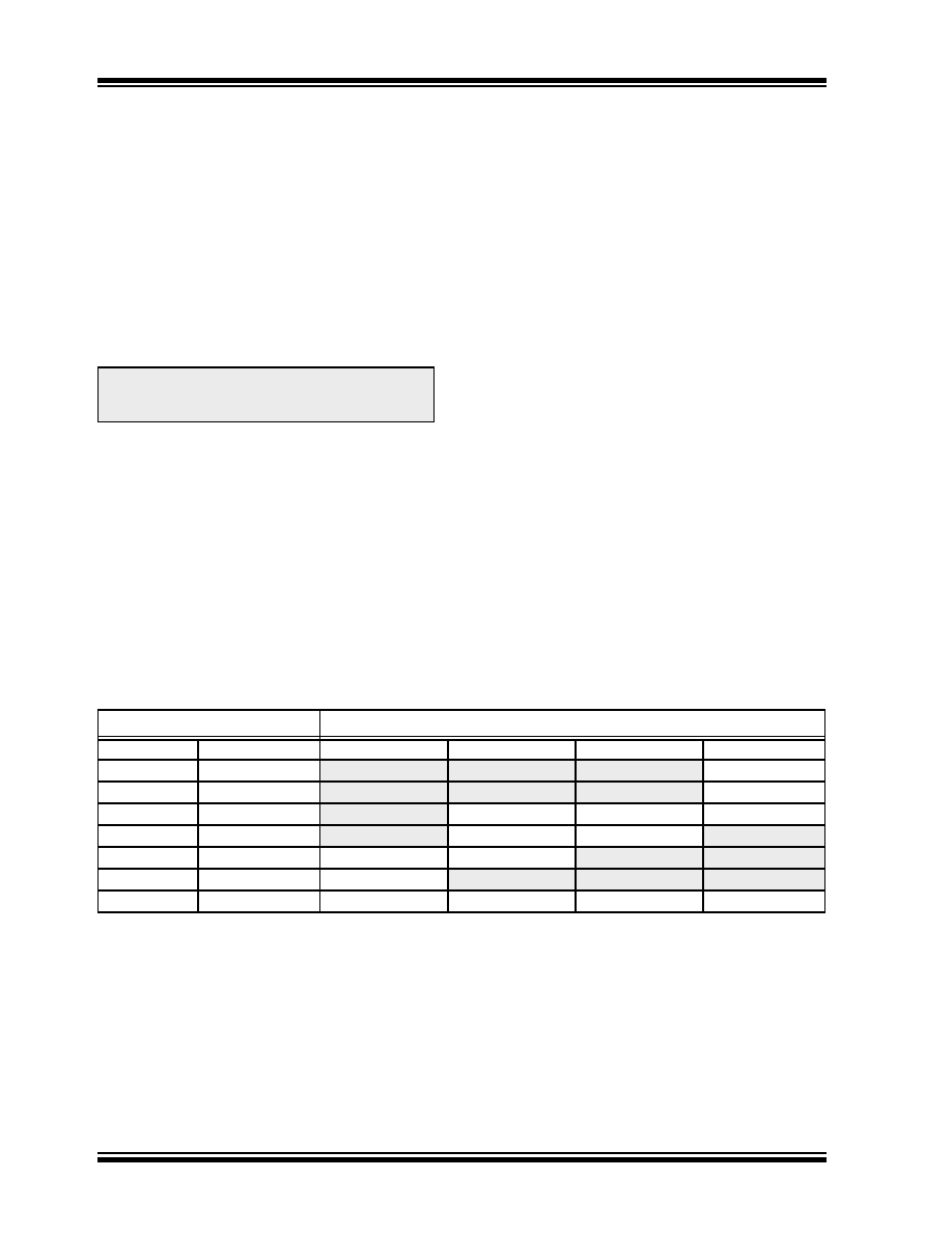
TABLE 12-1:
TAD vs. DEVICE OPERATING FREQUENCIES
Note:
Analog voltages on any pin that is defined
as a digital input may cause the input
buffer to conduct excess current.
A/D Clock Source (TAD)
Device Frequency
Operation
ADCS<2:0>
20 MHz
5 MHz
4 MHz
1.25 MHz
2 TOSC
000
100 ns(2)
400 ns(2)
500 ns(2)
1.6
μs
4 TOSC
100
200 ns(2)
800 ns(2)
1.0
μs(2)
3.2
μs
8 TOSC
001
400 ns(2)
1.6
μs2.0 μs6.4 μs
16 TOSC
101
800 ns(2)
3.2
μs4.0 μs
12.8
μs(3)
32 TOSC
010
1.6
μs6.4 μs
8.0
μs(3)
25.6
μs(3)
64 TOSC
110
3.2
μs
12.8
μs(3)
16.0
μs(3)
51.2
μs(3)
A/D RC
x11
2-6
μs(1,4)
2-6
μs(1,4)
2-6
μs(1,4)
2-6
μs(1,4)
Legend: Shaded cells are outside of recommended range.
Note 1:
The A/D RC source has a typical TAD time of 4
μs for VDD > 3.0V.
2:
These values violate the minimum required TAD time.
3:
For faster conversion times, the selection of another clock source is recommended.
4:
When the device frequency is greater than 1 MHz, the A/D RC clock source is only recommended if the
conversion will be performed during Sleep.
发布紧急采购,3分钟左右您将得到回复。
相关PDF资料
2-1546217-0
TERM BLK RCPT 20POS SIDE 5.08MM
1-1546217-9
TERM BLK RCPT 19POS SIDE 5.08MM
1-1546217-8
TERM BLK RCPT 18POS SIDE 5.08MM
1-1546217-7
TERM BLK RCPT 17POS SIDE 5.08MM
1-1546217-6
TERM BLK RCPT 16POS SIDE 5.08MM
1-1546217-5
TERM BLK RCPT 15POS SIDE 5.08MM
1-1546217-4
TERM BLK RCPT 14POS SIDE 5.08MM
1-1546217-3
TERM BLK RCPT 13POS SIDE 5.08MM
相关代理商/技术参数
ATMEGA169P-16MCU
功能描述:8位微控制器 -MCU AVR 16KB, 512B EE 16MHz 1KB SRAM, 5V
RoHS:否 制造商:Silicon Labs 核心:8051 处理器系列:C8051F39x 数据总线宽度:8 bit 最大时钟频率:50 MHz 程序存储器大小:16 KB 数据 RAM 大小:1 KB 片上 ADC:Yes 工作电源电压:1.8 V to 3.6 V 工作温度范围:- 40 C to + 105 C 封装 / 箱体:QFN-20 安装风格:SMD/SMT
ATMEGA169P-16MU
功能描述:8位微控制器 -MCU AVR 16K FLASH 512B EE 1K SRAM LCD ADC RoHS:否 制造商:Silicon Labs 核心:8051 处理器系列:C8051F39x 数据总线宽度:8 bit 最大时钟频率:50 MHz 程序存储器大小:16 KB 数据 RAM 大小:1 KB 片上 ADC:Yes 工作电源电压:1.8 V to 3.6 V 工作温度范围:- 40 C to + 105 C 封装 / 箱体:QFN-20 安装风格:SMD/SMT
ATMEGA169P-16MU SL383
制造商:Atmel Corporation 功能描述:MCU 8BIT ATMEGA RISC 16KB FLASH 3.3V/5V 64PIN MLF - Tape and Reel
ATMEGA169P-16MUR
功能描述:8位微控制器 -MCU AVR LCD 16KB FLSH EE 512B 1KB SRAM-16MHZ RoHS:否 制造商:Silicon Labs 核心:8051 处理器系列:C8051F39x 数据总线宽度:8 bit 最大时钟频率:50 MHz 程序存储器大小:16 KB 数据 RAM 大小:1 KB 片上 ADC:Yes 工作电源电压:1.8 V to 3.6 V 工作温度范围:- 40 C to + 105 C 封装 / 箱体:QFN-20 安装风格:SMD/SMT
ATMEGA169P-8AU
制造商:ATMEL 制造商全称:ATMEL Corporation 功能描述:Microcontroller with 16K Bytes In-System Programmable Flash
ATMEGA169P-8MU
制造商:ATMEL 制造商全称:ATMEL Corporation 功能描述:Microcontroller with 16K Bytes In-System Programmable Flash
ATMEGA169PA
制造商:ATMEL 制造商全称:ATMEL Corporation 功能描述:8-bit Microcontroller with 16K Bytes In-System Programmable Flash
ATMEGA169PA_1
制造商:ATMEL 制造商全称:ATMEL Corporation 功能描述:High Endurance Non-volatile Memory segments